


Infinite PCB.
High speed PCB Designs.
Infinite PCB.
IGES Provides hardware design services for electronics which includes high speed PCB design services with signal integrity and power integrity.
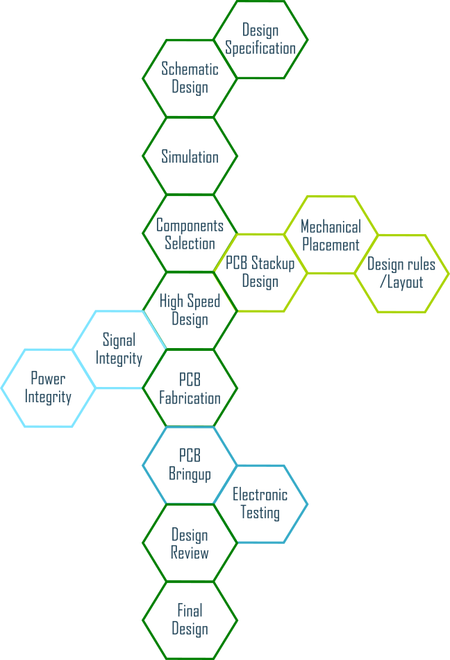
Infinite PCB Design Process.
Design Specifications:
Our PCB Design process starts with Design specifications. The specifications describe the intention form the electronic designs and identify the number of inputs, outputs, and the type of I/O signals from a voltage and current prospective. It also identifies the desired communication protocols and the sub systems that communicates with this system. We analyze that information and suggest MCU speed and memory size based on the application.
Schematic Design:
Next, we start our schematic design using PCB advanced software such as Altium Designer or similar software.
Simulation
The next step after the design is completed is to simulate the processes and the logic in the design. Simulation is critical to identify problems in the design beforehand.
Components Selection:
Once simulation is complete, we start the process of components selection. This process is particularly important to identify components that has acceptable tolerance based on the design specifications. We also recommend components in stock and available to mass produce as needed.
PCB Stackup Design:
PCB Stack up is critical specially for high-speed designs to take into consideration the desired impedance for conductors and the optimal design that can achieve signal and power integrity within the given design frequency.
Based on the design we can identify the number of layers, layers dimensions and thickness of copper and dialectic based on the materials used in the design. We can also design VIAS technology and PCB manufacturing technology. In addition, we can plan the layout of power and signals within the layers in addition to microstrips vs strip lines.
Mechanical Placement:
The mechanical layout is important to identify the shape of the PCB, packaging limitations and size limitation. It also helps identifying the location of communication and ports, terminals, and connectors. in addition, it allows to plan best approach of cooling the circuit and holes placement.
Design Rules:
Next, we start creating design rules, this can be limited by the design impedance, frequency/speed, current, temperature, and manufacturing technology. It is critical to have a reliable DRC that takes these rules into consideration.
We start the layout and wiring the PCB components based on the DRC and the design specs.
High Speed Design Power and Signal Integrity:
Now we can start fabrication, systems with high-speed signals requires exceptional design considerations from signal integrity and power integrity prospective. Every signal going through the PCB has to be planned out from speed, impedance prospective vs. conductor width and height. Selecting appropriate materials for the design is critical. Planning out the routs and separating power from high-speed signals is designed carefully. Signal such as bus, differential signals are treated different than single ended signals from signal integrity prospective. Cross talk, ground bounce and ESD and EMI can be sensed and cause a distortion in high-speed designs.
PCB Fabrication:
Fabrication can start next after selecting fabrication technology based on PCB type, material selection and Via technology. A good design can reduce the cost of fabrication exponentially.
GERBER files are generated next and so are Drill files in addition to 3D model and other documents such as schematic etc.
PCB Bringup:
PCB Bring up start by planning power sequences, checking impedance before powering the system and perform short circuit test and other appropriate tests. Once testing is performed and passed all steps it is documented.
Electronic Testing :
Design testing can be performed after hardware bring up and can be powered and connected to subsystems. Testing can incorporate hardware and software modifications.
Design Review:
Any problem is documented and then taken into a review process which can result in design modifications.
Final Design:
After performing all design modifications and documenting the design a final design is created and completed. Documentation is critical for successful designs and reliable products.

IGES provide a reliable electronics designs for various industries.
— IGES